- 您现在的位置:买卖IC网 > Sheet目录3841 > PIC18F86K22-I/PTRSL (Microchip Technology)MCU PIC 64K FLASH XLP 80TQFP
P89V52X2_3
NXP B.V. 2009. All rights reserved.
Product data sheet
Rev. 03 — 4 May 2009
31 of 57
NXP Semiconductors
P89V52X2
80C51 with 256 B RAM, 192 B data EEPROM
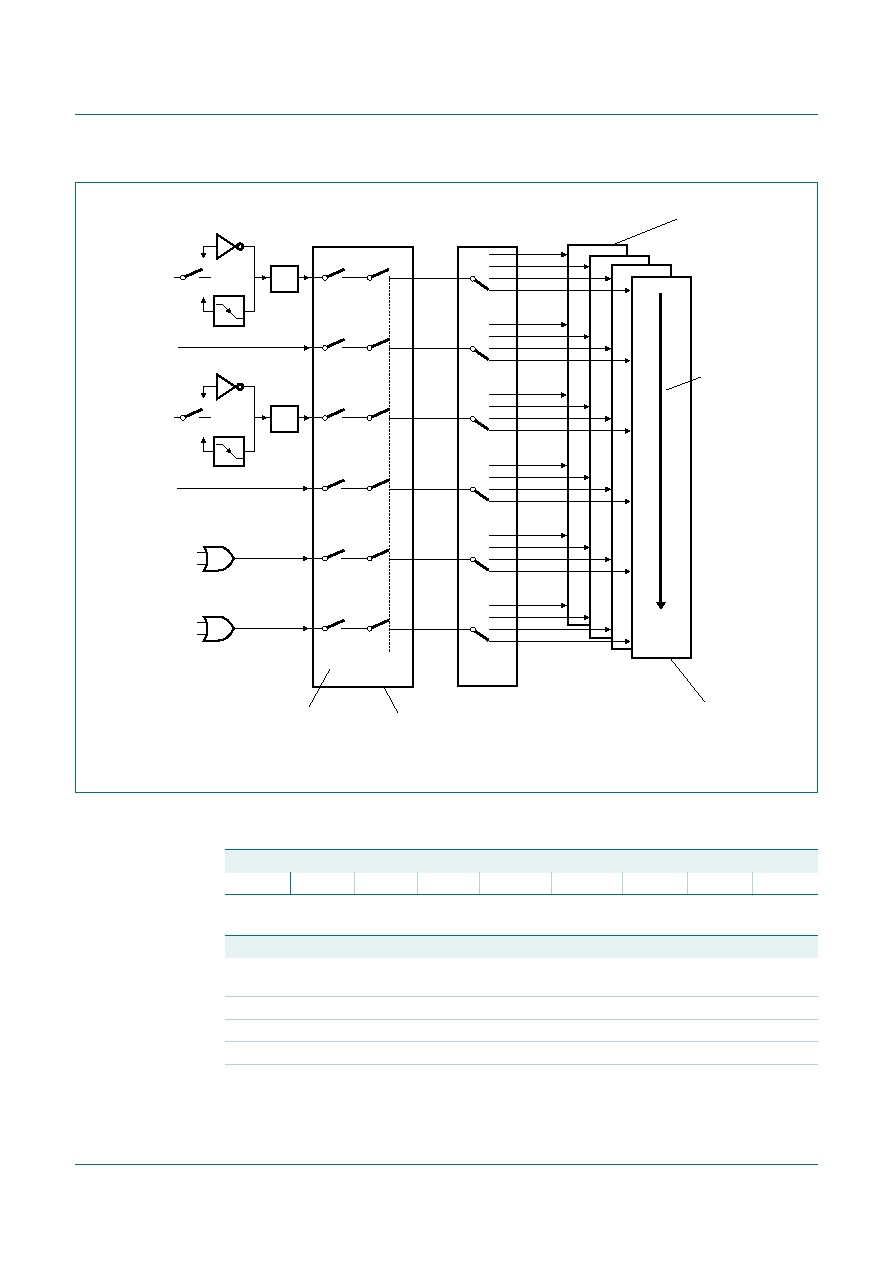
Fig 19. Interrupt structure
002aac568
highest
priority
interrupt
polling
sequence
INT0#
IE and IEA
registers
IP/IPH/IPA/IPAH
registers
individual
enables
global
disable
IE0
0
1
IT0
lowest
priority
interrupt
TF0
INT1#
TF1
RI
TI
TF2
EXF2
IE1
0
1
IT1
Table 25.
IE - Interrupt enable register (address A8H) bit allocation
Bit addressable; Reset value: 00H
Bit
7
6
5
4
3
2
1
0
Symbol
EA
-
ET2
ES
ET1
EX1
ET0
EX0
Table 26.
IE - Interrupt enable register (address A8H) bit description
Bit
Symbol
Description
7
EA
Interrupt Enable Bit: EA = 1 interrupt(s) can be serviced, EA = 0
interrupt servicing disabled.
6
-
Reserved
5
ET2
Timer 2 Overow Interrupt Enable
4
ES
Serial Port Interrupt Enable
3
ET1
Timer 1 Overow Interrupt Enable.
发布紧急采购,3分钟左右您将得到回复。
相关PDF资料
PIC16C63A-04I/SP
IC MCU OTP 4KX14 PWM 28DIP
PIC16C63A-04I/SO
IC MCU OTP 4KX14 PWM 28SOIC
52559-2270
CONN FFC 22POS .5MM VERT ZIF SMD
52559-1870
CONN FFC 18POS .5MM VERT ZIF SMD
DSPIC33EP64MC506-I/PT
IC DSC 16BIT 64KB FLASH 64TQFP
52745-1896
CONN FFC 18POS .5MM R/A ZIF SMD
PIC16LC622-04/P
IC MCU OTP 2KX14 COMP 18DIP
PIC16LF84A-04/P
IC MCU FLASH 1KX14 EE 18DIP
相关代理商/技术参数
PIC18F86K22-I/PTRSL
制造商:Microchip Technology Inc 功能描述:IC MCU 8BIT 64K FLASH 80TQFP ((NW)) 制造商:Microchip Technology Inc 功能描述:IC, 8BIT MCU, PIC18F, 16MIPS, TQFP-80
PIC18F86K22T-I/PT
功能描述:8位微控制器 -MCU 64kB Flash 4kB RAM
RoHS:否 制造商:Silicon Labs 核心:8051 处理器系列:C8051F39x 数据总线宽度:8 bit 最大时钟频率:50 MHz 程序存储器大小:16 KB 数据 RAM 大小:1 KB 片上 ADC:Yes 工作电源电压:1.8 V to 3.6 V 工作温度范围:- 40 C to + 105 C 封装 / 箱体:QFN-20 安装风格:SMD/SMT
PIC18F86K22T-I/PTRSL
功能描述:8位微控制器 -MCU 64KB Flash 4KB RAM nanoWatt XLP GP RoHS:否 制造商:Silicon Labs 核心:8051 处理器系列:C8051F39x 数据总线宽度:8 bit 最大时钟频率:50 MHz 程序存储器大小:16 KB 数据 RAM 大小:1 KB 片上 ADC:Yes 工作电源电压:1.8 V to 3.6 V 工作温度范围:- 40 C to + 105 C 封装 / 箱体:QFN-20 安装风格:SMD/SMT
PIC18F86K90-E/PT
功能描述:8位微控制器 -MCU 64KB Flash 4KB RAM LCD
RoHS:否 制造商:Silicon Labs 核心:8051 处理器系列:C8051F39x 数据总线宽度:8 bit 最大时钟频率:50 MHz 程序存储器大小:16 KB 数据 RAM 大小:1 KB 片上 ADC:Yes 工作电源电压:1.8 V to 3.6 V 工作温度范围:- 40 C to + 105 C 封装 / 箱体:QFN-20 安装风格:SMD/SMT
PIC18F86K90-I/PT
功能描述:8位微控制器 -MCU 64kB Flash 4kB RAM LCD
RoHS:否 制造商:Silicon Labs 核心:8051 处理器系列:C8051F39x 数据总线宽度:8 bit 最大时钟频率:50 MHz 程序存储器大小:16 KB 数据 RAM 大小:1 KB 片上 ADC:Yes 工作电源电压:1.8 V to 3.6 V 工作温度范围:- 40 C to + 105 C 封装 / 箱体:QFN-20 安装风格:SMD/SMT
PIC18F86K90-I/PTRSL
功能描述:8位微控制器 -MCU 64KB 4KB RAM 16MIPS nanoWatt XLP LCD 5V RoHS:否 制造商:Silicon Labs 核心:8051 处理器系列:C8051F39x 数据总线宽度:8 bit 最大时钟频率:50 MHz 程序存储器大小:16 KB 数据 RAM 大小:1 KB 片上 ADC:Yes 工作电源电压:1.8 V to 3.6 V 工作温度范围:- 40 C to + 105 C 封装 / 箱体:QFN-20 安装风格:SMD/SMT
PIC18F86K90T-I/PT
功能描述:8位微控制器 -MCU 64kB Flash 4kB RAM LCD
RoHS:否 制造商:Silicon Labs 核心:8051 处理器系列:C8051F39x 数据总线宽度:8 bit 最大时钟频率:50 MHz 程序存储器大小:16 KB 数据 RAM 大小:1 KB 片上 ADC:Yes 工作电源电压:1.8 V to 3.6 V 工作温度范围:- 40 C to + 105 C 封装 / 箱体:QFN-20 安装风格:SMD/SMT
PIC18F86K90T-I/PTRSL
功能描述:8位微控制器 -MCU 64KB 4KB RAM 16MIPS nanoWatt XLP LCD 5V RoHS:否 制造商:Silicon Labs 核心:8051 处理器系列:C8051F39x 数据总线宽度:8 bit 最大时钟频率:50 MHz 程序存储器大小:16 KB 数据 RAM 大小:1 KB 片上 ADC:Yes 工作电源电压:1.8 V to 3.6 V 工作温度范围:- 40 C to + 105 C 封装 / 箱体:QFN-20 安装风格:SMD/SMT